Memory
Memory
Stuff that needs to be remembered is data and it is held in memory • It can be stored, (modified) and retrieved for use
Physically there are several media on which we can store the data – the memory system – The choice comes down to speed, cost, power consumption, size etc.
A memory bit is “bistable”, i. e., stable in two positions either 0 or 1. • Each location is identified by its address, and it holds data. For our mbed both address and data are of 32 bits each.

计算机存储的原理
是这样一个电路
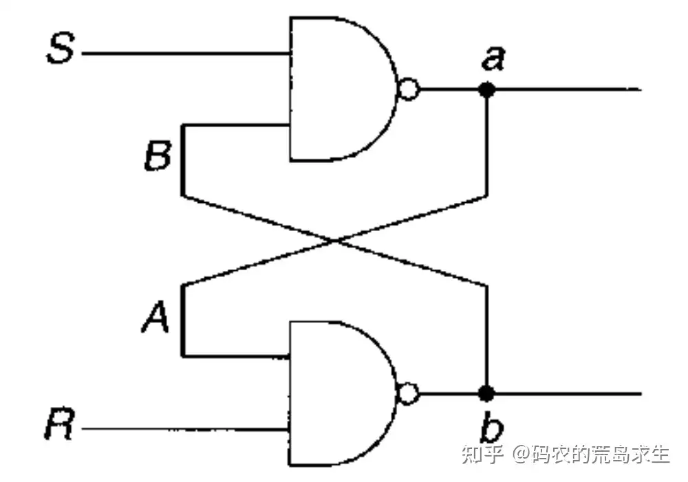
是两个NAND门(与非门)的组合,,先与然后取非,比如给定输入1和0,那么与运算后为0,非运算后为1
Volatile memory(易失性存储器)(RAM)
随机存取存储器(random access memory,RAM)又称作“随机存储器”,是与CPU直接交换数据的内部存储器,也叫主存(内存)。它可以随时读写,而且速度很快,通常作为操作系统或其他正在运行中的程序的临时数据存储媒介。
loses all data when power is removed, but is easy to write to.
- Volatile memory is traditionally used for data memory; it is essential to be able to write to memory easily, and there is little expectation for data to be retained when the product is switched off.
Ex. 主储存器,DRAM(动态随机存储器),快速CPU高速缓存存储器,Battery backed up static ram
*
| Static RAM (SRAM) | Dynamic RAM (DRAM) |
|---|---|
| Flip flops | Capacitor |
| It is static since it just stays put and remembers | It is dynamic since it loses it’s charge and has to be continually refreshed |
| More expensive&Low power consumption | Higher power consumption |
| Faster | Slower |
| Processor cache memory is usually SRAM | Computer RAM is usually DRAM |
| Slightly bigger area | Small area |
SRAM静态存储器
静态随机存取存储器(Static Random-Access Memory,SRAM)是随机存取存储器的一种。所谓“静态”指这种存储器只要保持通电,里面储存的数据就可以恒常保持,不需要周期性充电更新
工作原理: 利用双稳态触发器,存储元是用双稳态触发器(六管 MOS)来记忆信息的,即使信息被读出,它仍保持其原状态而不需要再生(非破坏性读出);只要电源被切断, 原来的保存信息便会丢失,它是易失性半导体存储器。
一般用来组成高速缓冲存储器Cache。
优点:
- 不需要刷新电路只要保持通电即能保存它内部存储的数据,因此具有较高的性能
- it is low power, can be written to and read from with ease, can be embedded onto a microcontroller, and hence forms the standard way of implementing data memory in most embedded systems.
局限性:
集成度较低,功耗比DRAM大,相同容量的DRAM可以设计为较小的体积,而SRAM却需要很大的体积。同样面积的硅片可以做出更大容量的DRAM,因此SRAM显得更贵
- These have to be addressable, so that just the right group of cells is written to, or read from, at any one time.
- To make this possible, two extra transistors are added to the two outputs.
- To reduce the power consumption, the two resistors are usually replaced by two transistors also. That means six transistors per memory cell
DRAM动态随机存取存储器
动态随机存取存储器(DRAM)里面所储存的数据就需要周期性地更新。 速度快,集成度低,高速缓冲存储器
intended to do the same thing as SRAM with a reduced silicon area.
Dynamic Random Access Memory,DRAM 是一种半导体存储器,主要是利用电容内存储电荷的多少来代表一个二进制比特是1还是0。由于在现实中晶体管会有漏电电流的现象,导致数据毁损,因此DRAM需要周期性地进行充电刷新
工作原理:
利用电容。电容中有电荷则存储的内容为1,没有电荷则表示内容为0,是利用存储元电路中栅极电容 上的电荷来存储信息的。【采用地址复用技术,地址线是原来的1/2,且地址信号分行、列两次传送
- Instead of using a number of transistors, one bit of information is stored in a tiny capacitor, like a small rechargeable battery.
- Such capacitors can be fabricated in large numbers on an IC.
- In order to select the capacitor for reading or writing, a simple transistor switch is required.
不足:
- Unfortunately, owing to the small capacitors and leakage currents on the chip, the memory loses its charge over a short period of time (around 10 to 100 ms). So the DRAM needs to be accessed every few milliseconds to refresh the charges, otherwise the information is lost.
- DRAM has about four times larger storage capacity than SRAM at about the same cost and chip size, with a compromise of the extra work involved in regular refreshing.
• It is, moreover, power hungry, so inappropriate for any battery-powered device. DRAM has found wide application as data memory in mains-powered computers, such as the PC.
Non-volatile memory (非易失性存储器)
retains its data when power is removed, but tends to be more complex to write to in the first place.
- Non-volatile memory is generally required for program memory, so that the program data is there and ready when the processor is powered up.
ex. 闪存,ROM,PROM,EPROM,FLASH等
ROM(Read-only memory)
只读内存(Read-Only Memory)是一种只能读取资料的内存。在制造过程中,将资料以一特制光罩(mask)烧录于线路中,其资料内容在写入后就不能更改,所以有时又称为“光罩式只读内存”(mask ROM)。此内存的制造成本较低,常用于电脑中的开机启动
The original ROMs and programmable read only memories (PROMs) could only ever be programmed once, and have now completely disappeared from normal usage. The first type of non-volatile reprogrammable semiconductor memory, electrically programmable read only memory (EPROM), represented a huge step forward:– A non-volatile memory could now be reprogrammed! With a process called hot electron injection (HEI), electrons can be forced through a very thin layer of insulator, onto a tiny conductor embedded within the insulator, and can be trapped there almost indefinitely.
工作特点:
非易失性存储器,工作时需要电源,当电源消失,存储的信息不会丢失
发展历程:
早期的只读存储器——在厂家就写好了内容,不可编写和更改
改进1——用户可以自己写——一次性编程不可擦除
改进2——可以多次写——能对信息进行擦除但不方便且擦除设备为另外特定设备
改进3——电可擦写——特定设备
改进4——电可擦写——直接连接在计算机上
常见ROM列举:
掩模ROM(MROM)不可编写和更改
PROM一次性编程
EPROM多次性编程,利用紫外线进行信息擦除,不方便
EEPROM多次性编程,电可擦写,可局部擦写也可全部擦写
FlashMemory闪速型存储器,有些设备可用它直接作硬盘,或者将它作为内存和硬盘间的缓冲
1.PROM
可编程程序只读内存(Programmable ROM,PROM)之内部有行列式的镕丝,视需要利用电流将其烧断,写入所需的资料,但仅能写录一次。 PROM在出厂时,存储的内容全为1,用户可以根据需要将其中的某些单元写入数据0(部分的PROM在出厂时数据全为0,则用 户可以将其中的部分单元写入1), 以实现对其“编程”的目的。PROM的典型产品是“双极性熔丝结构”,如果我们想改写某些单元,则可以给这些单元通以足够大的电流,并维持一定的时间,原 先的熔丝即可熔断,这样就达到了改写某些位的效果。另外一类经典的PROM为使用“肖特基二极管”的PROM,出厂时,其中的二极管处于反向截止状态,还 是用大电流的方法将反相电压加在“肖特基二极管”,造成其永久性击穿即可。
2.EPROM
可抹除可编程只读内存(Erasable Programmable Read Only Memory,EPROM)可利用高电压将资料编程写入,抹除时将线路曝光于紫外线下,则资料可被清空,并且可重复使用。通常在封装外壳上会预留一个石英透明窗以方便曝光。
- OTPROM
一次编程只读内存(One Time Programmable Read Only Memory,OPTROM)之写入原理同EPROM,但是为了节省成本,编程写入之后就不再抹除,因此不设置透明窗。
4.EEPROM
电子式可抹除可编程只读内存(Electrically Erasable Programmable Read Only Memory,EEPROM)之运作原理类似EPROM,但是抹除的方式是使用高电场来完成,因此不需要透明窗。
5.快闪存储器
快闪存储器(Flash memory)的每一个记忆胞都具有一个“控制闸”与“浮动闸”,利用高电场改变浮动闸的临限电压即可进行编程动作。
6.快闪存储器
指从游戏机主文件存储器里或者正版游戏卡带提取的游戏主文件,可以在各类模拟器上使用。例如街机模拟器,GBA模拟器的ROM,正是此意。
flash memory
Whole blocks have to be erased at any one time, ‘in a flash’.
This compromise leads to a huge advantage: flash memory is very high density indeed, more or less the highest available.
主要特性
- 需要先擦除再写入
Flash Memory 写入数据时有一定的限制。它只能将当前为 1 的比特改写为 0,而无法将已经为 0 的比特改写为 1,只有在擦除的操作中,才能把整块的比特改写为 1。 - 块擦除次数有限
Flash Memory 的每个数据块都有擦除次数的限制(十万到百万次不等),擦写超过一定次数后,该数据块将无法可靠存储数据,成为坏块。
为了最大化的延长 Flash Memory 的寿命,在软件上需要做擦写均衡(Wear Leveling),通过分散写入、动态映射等手段均衡使用各个数据块。同时,软件还需要进行坏块管理(Bad Block Management,BBM),标识坏块,不让坏块参与数据存储。(注:除了擦写导致的坏块外,Flash Memory 在生产过程也会产生坏块,即固有坏块。) - 读写干扰
由于硬件实现上的物理特性,Flash Memory 在进行读写操作时,有可能会导致邻近的其他比特发生位翻转,导致数据异常。这种异常可以通过重新擦除来恢复。Flash Memory 应用中通常会使用 ECC 等算法进行错误检测和数据修正。 - 电荷泄漏
存储在 Flash Memory 存储单元的电荷,如果长期没有使用,会发生电荷泄漏,导致数据错误。不过这个时间比较长,一般十年左右。此种异常是非永久性的,重新擦除可以恢复。
数据与内存
Data is transferred between memory and the rest of the system on buses. These are shared sets of wires that join the components, like a multi-lane highway. In the case of the 32 bit µC on the mbed, there are 32 parallel wires.
Several sets of these parallel wires are required :
• Address bus – carries address
• Data bus – carries the data bits either from the memory (read) or to the memory (write)
• Control lines are also needed to synchronise timing, select read/write, ensure that only one device tries to use the bus at once
计算机结构
冯·诺依曼结构(von Neumann architecture)
冯·诺依曼结构的处理器使用同一个存储器,经由同一个总线传输。冯·诺依曼结构处理器具有以下几个特点:
- 必须有一个存储器;
- 必须有一个控制器;
- 必须有一个运算器,用于完成算术运算和逻辑运算;
- 必须有输入和输出设备,用于进行人机通信。
哈佛结构(Harvard Architecture)
一种将程序指令存储和数据存储分开的存储器结构
央处理器首先到程序指令存储器中读取程序指令内容,解码后得到数据地址,再到相应的数据存储器中读取数据,并进行下一步的操作(通常是执行)。程序指令存储和数据存储分开,可以使指令和数据有不同的数据宽度
与冯.诺曼结构处理器比较,哈佛结构处理器有两个明显的特点:
(1).使用两个独立的存储器模块,分别存储指令和数据,每个存储模块都不允许指令和数据并存;
(2).使用独立的两条总线,分别作为CPU与每个存储器之间的专用通信路径,而这两条总线之间毫无关联。
后来,又提出了改进的哈佛结构,其结构特点为:
(1).使用两个独立的存储器模块,分别存储指令和数据,每个存储模块都不允许指令和数据并存;
(2).具有一条独立的地址总线和一条独立的数据总线,利用公用地址总线访问两个存储模块(程序存储模块和数据存储模块),公用数据总线则被用来完成程序存储模块或数据存储模块与CPU之间的数据传输;
(3).两条总线由程序存储器和数据存储器分时共用。
Memory-Mapped Input/Output I/O
内存映射输入输出
存储器映射就是为物理内存按一定编码规则分配地址的行为
This is the most common way of treating the input/output ports.
– I/O ports are connected like memory
– I/O ports are assigned addresses
– Software accesses I/O using reads and writes to the specific I/O addresses
The same instructions are used for accessing I/O ports and memory
– Inputs from an input device: same instructions as a memory read
– Outputs to an output device: same instructions as a memory write
Easier to design, and software is easier to write
I/O-mapped I/O (used in older Intel devices)
– The control bus signals that activate the I/O are separate from those that activate the memory devices
– Separate address space
– Separate instructions to access the I/O devices
– Software can not without intention access I/O when it thinks it is accessing memory